I/O modules
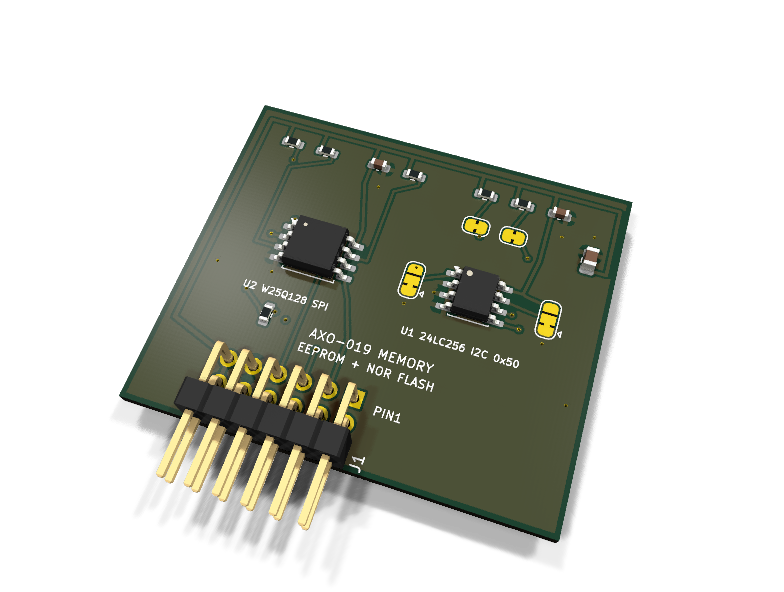
AXO-019 — Memory sampler PMOD module (I2C EEPROM + SPI NOR flash)
Catalog #19 in the AruviX output line, level L3. Two non-volatile memories on one PMOD so the technologies can be contrasted side by side, on both serial buses at once.
Circuit review & bench-test guide →
Components#
Every placed component, with the reason it is on the board. Extracted directly from the schematic, so this cannot drift from the design.
| Ref | Value | What it does on this board | Part number | Footprint |
|---|---|---|---|---|
C1 |
100nF 16V X7R | U1 EEPROM decoupling | GRM188R71C104KA01DMurata |
C_0603_1608Metric |
C2 |
100nF 16V X7R | U2 flash decoupling | GRM188R71C104KA01DMurata |
C_0603_1608Metric |
C3 |
10uF 10V X5R | Bulk reservoir for flash program/erase current | GRM21BR61A106KE19LMurata |
C_0805_2012Metric |
J1 |
PMOD PLUG 2x6 | PMOD peripheral plug (Digilent spec 1.2) | not selected generic |
PinHeader_2x06_P2.54mm_Horizontal |
JP1 |
SDA PULL-UP | Cut to remove the SDA pull-up when chaining modules | — | SolderJumper-2_P1.3mm_Bridged_RoundedPad1.0x1.5mm |
JP2 |
SCL PULL-UP | Cut to remove the SCL pull-up when chaining modules | — | SolderJumper-2_P1.3mm_Bridged_RoundedPad1.0x1.5mm |
JP3 |
A0 0x50/0x51 | EEPROM address: 1-2 A0 low 0x50 (default), 2-3 A0 high 0x51 (A1/A2 tied low) | — | SolderJumper-3_P1.3mm_Bridged12_RoundedPad1.0x1.5mm |
JP4 |
WP OFF/ON | EEPROM write protect: 1-2 WP low = writable (default), 2-3 WP high = write-protected | — | SolderJumper-3_P1.3mm_Bridged12_RoundedPad1.0x1.5mm |
R1 |
4.7k | I2C SDA pull-up | RC0603FR-074K7LYageo Datasheet ↗ |
R_0603_1608Metric |
R2 |
4.7k | I2C SCL pull-up | RC0603FR-074K7LYageo Datasheet ↗ |
R_0603_1608Metric |
R3 |
100R | Series protection on the flash-driven MISO line | RC0603FR-07100RLYageo Datasheet ↗ |
R_0603_1608Metric |
R4 |
10k | ~WP pull-up: status-register writes allowed; IO2 idle high for future quad use | RC0603FR-0710KLYageo Datasheet ↗ |
R_0603_1608Metric |
R5 |
10k | ~HOLD pull-up so a floating host cannot pause the flash mid-transfer | RC0603FR-0710KLYageo Datasheet ↗ |
R_0603_1608Metric |
R6 |
10k | ~CS idle pull-up so the flash stays deselected before FPGA config | RC0603FR-0710KLYageo Datasheet ↗ |
R_0603_1608Metric |
U1 |
24LC256 | 32 KB I2C EEPROM, byte/page writable, addr 0x50/0x51 via A0 | 24LC256-I/SNMicrochip Datasheet ↗ |
SOIC-8_3.9x4.9mm_P1.27mm |
U2 |
W25Q128JVS | 128 Mbit (16 MB) SPI NOR flash, 208-mil SOIC-8, ECP5 boot-flash family | W25Q128JVSIQWinbond Datasheet ↗ |
SOIC-8_5.3x5.3mm_P1.27mm |
Signals#
Net labels used in the schematic, which are also the names the HDL top level should use.
3V3 CS_N EE_A0 EE_WP FLASH_DO FLASH_HOLD_N FLASH_WP_N GND MISO MOSI SCK SCL SCL_PU SDA SDA_PU
Production status#
| Schematic ERC | 0 violations |
|---|---|
| PCB layout | complete |
| DRC | 0 violations |
| Fab package | exported (24 gerbers + drill + CPL + BOM) |
| Fabricated | no — design stage only |
Source: boards/io-modules/axo-019-memory
Catalog #19 in the AruviX output line (../README.md), level L3. Two non-volatile memories on one PMOD so the technologies can be contrasted side by side, on both serial buses at once.
Status: schematic generated, ERC clean (0/0), netlist reviewed. PCB layout not started. Not released.
What it teaches#
Byte-writable EEPROM vs page/sector NOR flash — the core non-volatile storage contrast:
- 24LC256 (I2C, 32 KB): rewrite any single byte in place (~5 ms write cycle), 64-byte page writes, ~1 M erase/write cycles. Storage that behaves like slow RAM.
- W25Q128JV (SPI, 16 MB): programming only clears bits 1→0 in 256-byte pages; going back to 1 means erasing a whole 4 KB sector; ~100 k cycles. Big and cheap, but the program/erase asymmetry forces wear-levelling and log-structured thinking.
The flash is the same W25Q family the ECP5 host boots from, so the SPI flash driver written here is literally the boot-flash driver for the platform (and for AruviOS's flashrom-style tooling).
Catalog note: the catalog line said W25Q64; the stock KiCad symbol set carries the W25Q128JVS, so the fitted part is the 128 Mbit W25Q128JVSIQ (same command set, one more capacity bit).
Design#
- Hybrid pin map like the axo-010 DAC board: SPI (Type 2) on pins 1/2/3/4 for the flash, I2C on pins 9/10 — the line's bus-repeat positions — for the EEPROM. Both memories usable simultaneously.
- EEPROM (U1, 24LC256-I/SN, SOIC-8):
- A0 on solder jumper JP3: default bridged to GND = 0x50; bridge 2-3 to VDD for 0x51 (lets two of these boards chain on one bus). A1/A2 tied to GND.
- WP on solder jumper JP4: default bridged to GND = writable; bridge 2-3 to VDD = write-protected.
- Standard I2C pattern: 4.7 k pull-ups via JP1/JP2 (cut when the chain already has pull-ups), nets
SDA_PU/SCL_PU. - Flash (U2, W25Q128JVSIQ, SOIC-8 208 mil): stock symbol
Memory_Flash:W25Q128JVSwith its default stock footprintPackage_SO:SOIC-8_5.3x5.3mm_P1.27mm(the 208-mil wide body — verified). - ~CS / DI / DO / CLK on PMOD 1/2/3/4; flash-driven DO passes 100 R (R3).
- ~WP and ~HOLD: 10 k pull-ups (R4/R5) — plain SPI, status register writable, no accidental mid-transfer hold; quad mode not wired this rev.
- ~CS 10 k pull-up (R6) keeps the flash deselected before FPGA config.
- 100 nF per IC + 10 µF bulk for program/erase current.
| PMOD pin | 1 | 2 | 3 | 4 | 5 | 6 | 7 | 8 | 9 | 10 | 11 | 12 |
|---|---|---|---|---|---|---|---|---|---|---|---|---|
| Net | ~CS | MOSI (DI) | MISO (DO) | SCK | GND | 3V3 | NC | NC | SCL | SDA | GND | 3V3 |
Regenerate#
python3 generate_design.pyRemaining for release#
- [ ] PCB layout, DRC, fab outputs
- [ ]
hdl/: I2C EEPROM read/write demo, SPI flash JEDEC-ID + read/program/erase demo, side-by-side "write a byte" lesson bench - [ ] BOM export and availability check, design-review checklist